관련 논문 “LightNVM: The Linux Open-Channel SSD Subsystem”
Abstraction
예측 가능성에 대한 요구사항이 있음. Block I/O를 하는 SSD는 왜 unpredictable 하지? LightNVM integrates into tra- ditional storage stack. 여기서 traditional storage stack이 뭔지 아직 모르겠음.
LightNVM 은 예측가능한 Latency를 갖는다.
1. introduction
These shortcomings are not due to hardware limitations: the non-volatile memory chips at the core of SSDs provide predictable high-performance at the cost of constrained operations and limited en- durance/reliability. It is how tens of non-volatile memory chips are managed within an SSD, providing the same block I/O interface as a magnetic disk, which causes these shortcomings
Open-Channel SSD: They are an excellent plat- form for addressing SSD shortcomings and managing trade-offs related to throughput, latency, power con- sumption, and capacity.
There are two concerns here: (1) a block device abstraction implemented on top of open- channel SSDs should provide high performance, and (2) design choices and trade-off opportunities should be clearly identified.
LightNVM is the first open, generic subsystem for Open- Channel SSDs and host-based SSD management.
여기서 말하는 host-based에서 host는 PC환경을 말하는 것인가? - > 운영체제! (여기서는 리눅스 드라이버를 말함)
4 contribution
First, we describe the character- istics of open-channel SSD management.
Second, we introduce the Physical Page Address (PPA) I/O interface, an interface for Open-Channel SSDs, that defines a hierarchical address space together with control and vectored data commands.
Third, we present LightNVM, the Linux subsystem that we designed and implemented for open-channel SSD management.
Finally, we demonstrate the effectiveness of Light- NVM on top of a first generation open-channel SSD.
Our results show that LightNVM achieves high performance and can be tuned to control I/O latency variability.
2. Open-Channel SSD Management
2.1 NAND Flash Characteristics
구조적으로 셀 들이 직렬 단위로 연결되어 있고, 주소 라인이 없기 때문에 라인에 맞춰 읽기, 쓰기 및 지우기 작업을 진행한다. 따라서 다음과 같이 세 가지 작업을 할 수 있음.
- 읽기 - 페이지 단위로 작업
- 쓰기 - 페이지 단위로 작업
- 지우기 - 블록 단위로
이렇게 낸드 플래시 메모리는 페이지 단위로 읽기 작업을 진행하기 때문에 단 1Byte 의 데이터를 읽고자 할 지라도 우선 해당 데이터가 포함된 페이지 전체를 통채로 읽은 후, 필요한 데이터를 따로 추출하는 방식을 사용한다.
또한 이러한 작업 구조와 덮어쓰기가 불가능한 셀의 특성으로 인해 단 한 1Byte 의 데이터를 바꾸는 경우라도 먼저 블록 전체를 지우고, 해당 블록 내의 모든 페이지를 다시 써야만 하는 문제가 발생하게 된다. 이것은 특히나 문제가 되는데, SSD 에서는 이러한 문제를 해결하기 위해 플래시 변환 계층(FTL)을 통한 웨어 레벨링(Wear Leveling)을 통해 이 문제를 해결함.
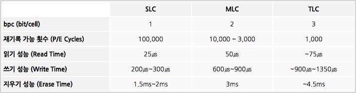
SLC, MLC, TLC
| 방식 | 특징 | ex |
|---|---|---|
| SLC | 하나의 셀에 1bit를 저장 | 0, 1 |
| MLC | 하나의 셀에 2bit를 저장 | 00, 01, 10, 11 |
| TLC | 하나의 셀에 3bit를 저장 | 000, 001, 010, 011, 100, 101, 110, 111 |
성능과 수명은 SLC > MLC > TLMC 순서로 좋고 가격은 그의 역순이다. 왜냐하면 세 가지 SSD방식에서 사용하는 셀은 완전히 동일한데 비해 저장하는 bit는 1, 2, 3으로 각각 1배, 2배, 3배로 차이가 나기 때문. 따라서 SLC, MLC, TLC 낸드 플래시 메모리가 서로 동일한 크기일 때, 이론적으로 SLC 에 비해 MLC 는 2 배의 용량을, TLC 는 3 배의 용량을 가진다.
2.2 Manageing NAND
Write Buffering
if the sector size, host-size defined, is smaller than the NANA Flash page size(eg. 4KB sector size, 16KB flash page), *write buffeing is necessary**
전통적인 해결 방법:
using cache - sector write is buffered until enough data is gathered to fill flash page. flush 와 같이 write가 강제되어야 할 경우 padding. Read가 있을 경우 cache에서 바로 읽는다.
장, 단점:
If the cache resides on the host, then the two advantages are that (1) writes are all generated by the host, thus avoiding interference between the host and devices, and that (2) writes are acknowledged as they hit the cache. The disadvantage is that the contents of the cache might be lost in case of a power failure.
Two way to write:
- The write cache may also be placed on the device side. Either the host writes sectors to the device and lets the device manage writes to the media (when enough data has been accumulated to fill a flash page) - controller-generated writes 가 발생할 수 있기 때문에 workload를 unpredictable하게 할 수 있다.(???)
- the host explicitly controls writes to the media and lets the device maintain durability - host has full control of media operations
Error Handling
ECC:
To compensate for bit errors, it is necessary to introduce Error Correcting Codes (ECC), e.g., BCH [53] or LDPC [16]. Typically, the unit of ECC encoding is a sector, which is usually smaller than a page. ECC parities are generally handled as metadata associated with a page and stored within the page’s out-of-band area.
BER:
To maintain BER below a given threshold, some vendors make it possible to tune NAND threshold voltage [7, 8]. Blocks which are write-cold and read-hot, for which BER is higher than a given threshold, should be rewritten
read dominant한 access를 갖을 때, 왜 rewritten되어야 하지??
Workload and RAID: Note that different workloads might require different RAID configurations. Typically, high read workloads re- quire less redundancy, because they issue fewer PE cycles. This is an argument for host-based RAID implementation. Conversely, for high write workloads, RAID is a source of overhead that might be compensated by hardware acceleration
Write failure: In the case of write failures, due to overcharging or inherent failures [51], recovery is necessary at the block level. When a write fails, part of a block might already have been written and should be read to perform recovery
Erase failure: If a failure occurs on erase, there is no retry or recovery. The block is simply marked bad.
2.3 Lessons Learned
Provide device warranty with physical access.
P/E cycle은 write operation에 영향. To provide warranty, PE cycles must be managed on the device
Exposing media characterization to the host is inefficient and limits media abstraction
embedded FTL을 NAND Flash에 맞춰서 characterization 하는 것은 바람직 하지 않다.
Write buffering should be handled on the host or the device depending on the use case.
host-side: 만약 호스트가 write buffering을 Handling한다면, SSD에 dram이 필요 없을 수 있고, 소비전력도 줄어들 수 있다.
device-side: Managing the write buffer on the device, through a CMB, efficiently supports small writes but requires ex- tra device-side logic, together with power-capacitors or similar functionality to guarantee durability. Both op- tions should be available to open-channel SSD vendors.
Application-agnostic wear leveling is mandatory.
To make sure that latency does not fluctuate depending on the age of the block accessed, it is mandatory to perform wear-leveling independently from the application workload, even if it introduces an overhead
It must be possible, either for the host or the controller, to pick free blocks from a die in a way that (i) hides bad blocks, (ii) implements dynamic wear leveling by taking the P/E cycle count into account when allocating a block, and possibly (iii) implements static wear level- ing by copying cold data to a hot block.
위와 같은 3가지 방법은 메타데이터(P/E cycle per block, read counts per page, and bad blocks 등)에 의해 결정할 수 있다. 이러한 블록 메타데이터를 관리하는 것 또한 오버헤드가 발생함.
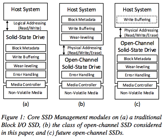
2.4 Architecture
3. Physical Page Address I/O interface
Address space
- SSD Architecture. Open-channel SSDs expose to the host a collection of channels, each containing a set of Parallel Units (PUs), also known as LUNs. We define a PU as the unit of parallelism on the device. A PU may cover one or more physical die, and a die may only be a member of one PU. Each PU processes a single I/O request at a time.
- Media Architecture. Regardless of the media, storage space is quantized on each PU. NAND flash chips are decomposed into blocks, pages (the minimum unit of transfer), and sectors (the minimum unit of ECC). Byte-addressable memories may be organized as a flat space of sectors.
NAND Flash memory 구조
다음은 NAND Flash memory 구조를 나타내는 예시로서 「2 Die - 2 Plane」 의 구조를 가진 8GB(64Gb) 낸드 플래시 메모리 이다. 「1 Plane = 1,024 Block」 「1 Block = 256 Page」 「1 Page = 8KB」 로 구성
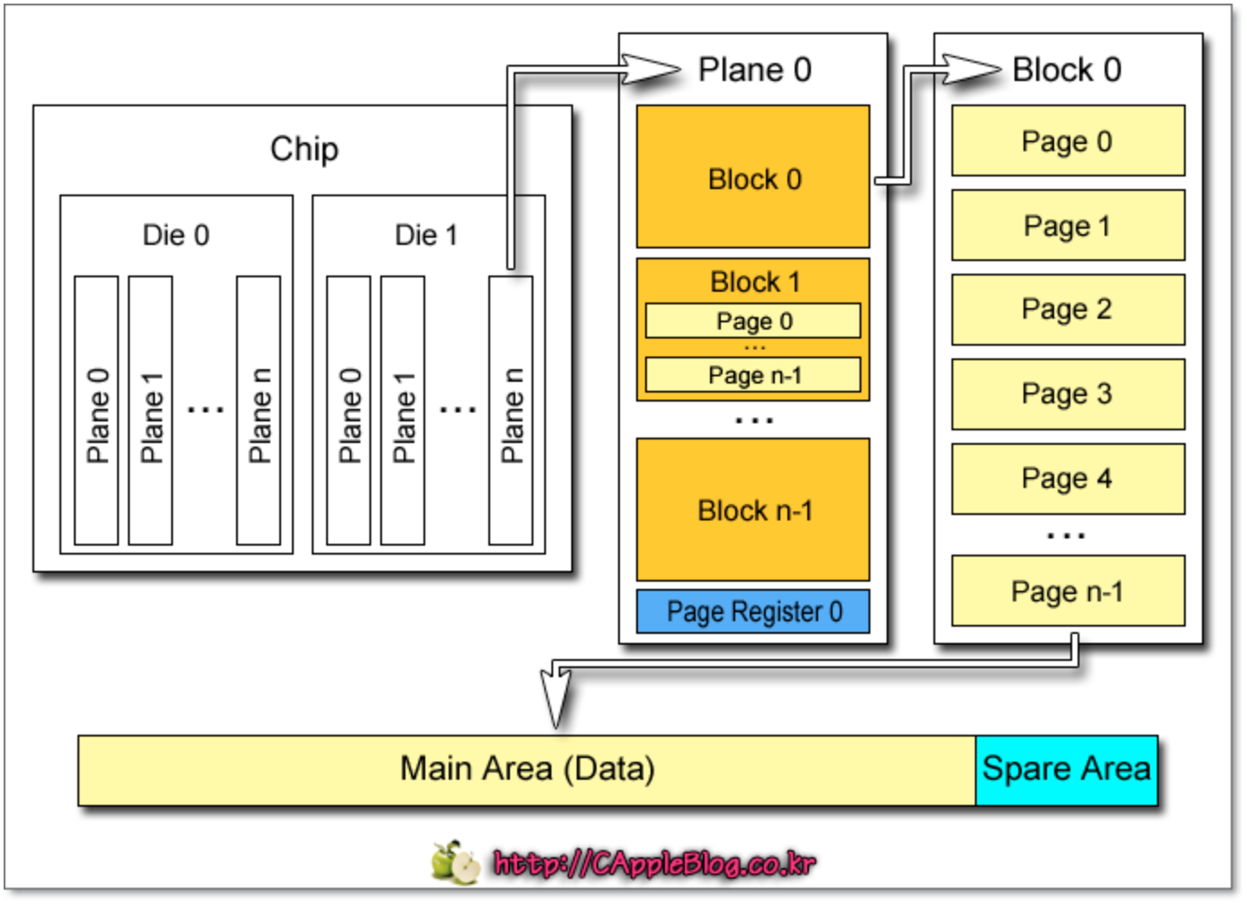
본 논문에서는 PU는 하나의 physical NAND die라고 가정함.
- PPA를 쓰는 이유, 장점 Encoding the SSD and media architecture into physical addresses makes it possible to define hardware units, embedded on an open-channel SSD, that map incoming I/Os to their appropriate physical placement. The PPA format is also well-suited for a representation where the identifiers are independent variables as a power of two. This way, operations on the namespace (e.g., get next page on the next channel, or get next page on a different PU) are efficiently implemented by shifting bits.
3.2 Geometry and Management
host가 SSD에 대한 관리를 통제하기 위해서 open- channel SSD 는 다음과 같은 네 가지 특징을 보인다.
- 수학적 특징: Its geometry, i.e., the dimensions of the PPA address space. How many channels? How many PUs within a channel? How many planes per PU? How many blocks per plane? How many pages per block? How many sectors per page? How large is the out-of-bound region per page? We assume that PPA dimensions are uniform for a given address space. If an SSD contains different types of storage chips, then the SSD must expose the storage as separate address spaces, each based on similar chips.
- 성능적 특징: Its performance, i.e., statistics that capture the performance of data commands, channel capacity and controller overhead. The current version of the specification captures typical and max latency for page read, page write, and erase commands and the maximum number of in-flight commands addressed to separate PUs within a channel.
- 저장매체와 관련된 메타데이터: Media-specific metadata. For instance, NAND flash-specific metadata includes the type of NAND flash on the device, whether multi-plane operations are supported, the size of the user-accessible out-of- bound area, or page pairing information for MLC and TLC chips. As media evolves, and becomes more complex, it may be advantageous to let SSDs handle this complexity.
- SSD 컨트롤러의 기능: Controller functionalities. As we have seen in Section 2, a controller might support write buffering, failure handling, or provisioning. Each of these capabilities might be configured (e.g., RAID across PUs). If the controller supports write buffering, then a flush command enables the host to force the con- troller to write the contents of its buffer to the storage media.
- over provisioning: 웨어레벨링이나 가비지 컬렉션은 SSD에 어느정도 여유공간이 있을 때, 원활하게 작동한다. 따라서 SSD의 저장 공간이 대부분 차지되었을 경우에도 원활한 작동을 위해 여분의(사용자에게는 보여지지 않는) over provisioning space가 존재한다.
3.3 Read/Write/Erase
Vectored I/Os: a read or write is applied to a vector of addresses to leverage the intrinsic parallelism of the SSD. For example, let us consider 64KB of application data. Assuming a page size of 4KB, this data might be striped with a write command applied to 16 sectors simultaneously, thus efficiently supporting scattered access.
다음과 같은 세 가지 방법을 고려했음, -> (i) NVMe I/O command, (ii) grouped I/Os, and (iii) Vectored I/Os. Vectored I/O에서는, an extra DMA is required to communicate the PPA list.
Media specific: The plane operation mode defines how many planes should be programmed at once. The controller may use the plane operation mode hint to efficiently program planes in parallel, as it accesses PUs sequentially by default. Similarly, the erase-suspend al- lows reads to suspend an active write or program, and thus improve its access latency, at the cost of longer write and erase time.
4. LightNVM
4.1 Architecture
LightNVM is the open-channel SSD subsystem in Linux
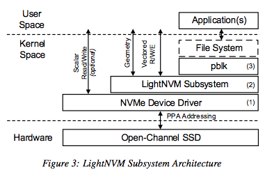
NVMe Device Driver: A LightNVM-enabled NVMe device driver gives kernel modules access to open-channel SSDs through the PPA I/O interface.
LightNVM Subsystem:
???
High-level I/O Interface: High-level I/O Interface를 통해서 커널-영역의 모듈이나 유저-영역의 어플리케이션 접근을 Open-Channel SSDs에 준다.
4.2 pblk
pblk이 하는 일: pblk’s main responsibilities are to (i) deal with controller- and media-specific constraints (e.g., caching the necessary amount of data to program a flash page), (ii) map logical addresses onto physical addresses (4KB granularity) and guarantee the integrity—and eventual recovery in the face of crashes—of the associated mapping table (L2P), (iii) handle errors, and (iv) implement garbage collection (GC). Since typical flash page sizes are bigger than 4KB, pblk must also (v) handle flushes. A flush forces pblk’s in-flight data to be stored on the device before it completes. It might be required by a file system or an application (i.e., fsync).
Producer & Consumer
4.2.2 Mapping Table Rocovery
data consistency를 위해 L2P mapping table redundant 하게 유지 해야한다. 다음과 같이 세 가지 방법을 통해서;
First, as a snapshot, which is stored (i) on power-down, in form of a full copy of the L2P, and (ii) periodically as checkpoints in form of an FTL log that persists operations on blocks (allocate and erase).
Second, as block-level metadata, on the first and last page of each block. When a block is opened, the first page is used to store a block sequence number together with a reference to the previous block. When a block is fully written, the last pages are used to store (1) an FTL-log consisting of the portion of the L2P map table corresponding to data in the block, (2) the same sequence number as in the first page in order to avoid an extra read during recovery, and (3) a pointer to the next block. The number of pages needed depends on the size of the block.
Finally, a portion of the mapping table is kept (iii) within the OOB area of each flash page that is written to the device
To ensure data correctness, it is paramount that half- written lower/upper pages are padded before reads can be issued. If the controller counts on a super capacitor, padding can be done in the device on ungraceful power- down. Otherwise, padding must be implemented on the second phase of recovery, as partially written blocks are recovered.
4.2.3 Error Handling
Unlike a traditional FTL that deals with read, write, and erase failures, pblk deals only with write and erase errors.
recovery must be managed by the upper layers of the system, above pblk.
When a write fails, pblk initiates two recovery mechanisms.
In the case of erase failures, the block is directly marked as bad. Since no writes have been issued at this point, there is no data to recover.
4.2.4 Garbage Collection
Therefore, pblk simply maintains a valid page count for each block, and selects the block with the lowest number of valid sectors for recycling.
The reverse logical to physical mapping table is not stored in host memory. To find a reverse mapping, we leverage the fact that a block is first recycled when it is fully written. Thus, we can use the partial L2P table stored for recovery on the last pages of the block
To prevent user I/Os from interfering with garbage collection, pblk implements a PID controlled [44] rate- limiter, whose feedback loop is based on the total number of free blocks available.
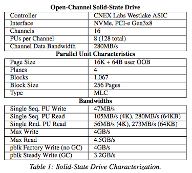
5. Experiment Evaluation